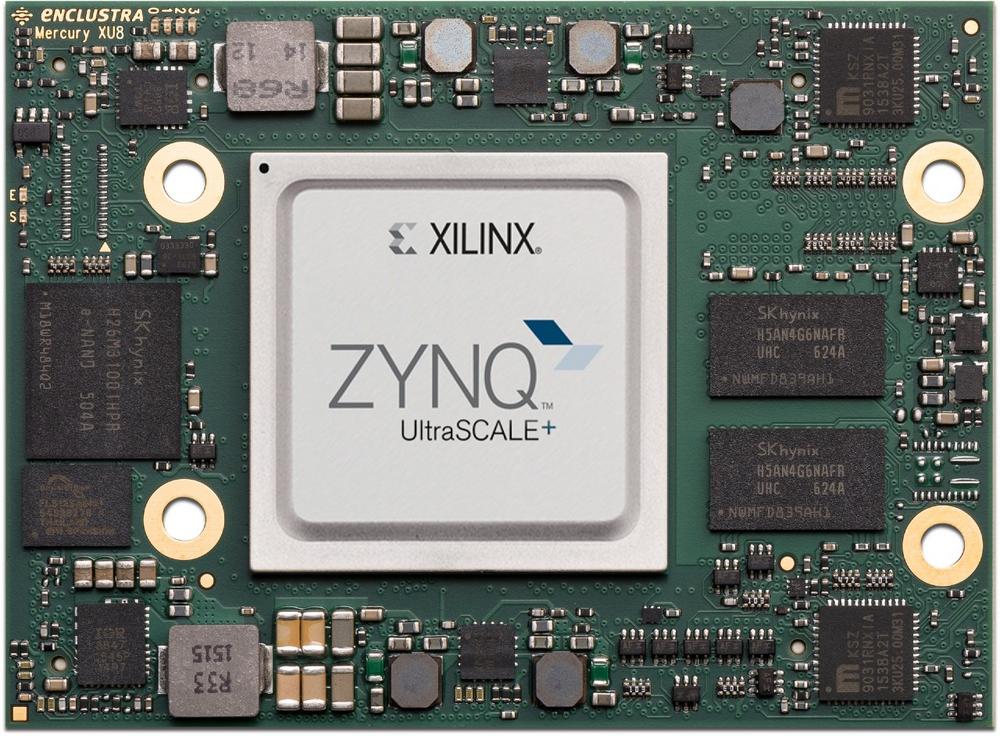
The Mercury+ XU8 MPSoC module from FPGA specialist Enclustra is optimized for applications that need to process large amounts of data in the shortest possible time. With two independent memory channels – one on the PS (up to 8 GByte DDR4 ECC SDRAM) and one on the PL (up to 4 GByte) – the module achieves a memory bandwidth of up to 29.8 GByte/sec. In order to transport the data to be processed into and out of the module as quickly as possible, 20 multi-gigabit transceivers with a data transmission rate of up to 15 Gbit/sec each are available.
The module is available in both commercial and industrial temperature ranges, needs just a single 5-15 V supply for operation and has a planned availability of 10 years.
In addition to the usual standard interfaces such as Gigabit Ethernet, USB 3.0, Display Port, SATA and SGMII, the 74 × 54 mm small module has a 16 GByte eMMC and a 64 MByte QSPI Flash. Both the processing system and the FPGA matrix have PCIe® connections.
The Xilinx Zynq UltraScale+ MPSoC is manufactured in a 16 nm FinFET+ process and has 6 ARM® cores: four 64 bit ARM Cortex™-A53 with a clock frequency of up to 1333 MHz and a 600 MHz fast 32 bit ARM® dual core Cortex™-R5. The processors are supported by a Mali™-400MP2 GPU and a H.264/H.265 video codec (EV variants).
Reference design and Linux at the push of a button
Enclustra offers a broad design-in support for their products. With the Mercury+ PE1-300 or Mercury+ PE1-400 baseboards, the Mercury+ XU8 can be a powerful development and prototyping platform.
Further expansion options are provided by the LPC/HPC FMC connectors on the PE1 base board, compatible with a huge range of plug-in cards from various manufacturers – ADCs, DACs, motor control cards and RF links are just a small selection of possibilities.
Enclustra also offers a comprehensive ecosystem for the XU8, offering all required hardware, software and support materials. The Mercury+ PE1 base board is a complete development platform; detailed documentation and reference designs make it easy to get started, in addition to the user manual, user schematics, a 3D-model, PCB footprint and differential I/O length tables.
The Enclustra Build Environment can be used to compile the Enclustra SoC modules with an integrated ARM processor very smoothly. The module and base board are selected by a graphical interface. After that, the Enclustra Build Environment downloads the appropriate Bitstream, First Stage Boot Loader (FSBL) and the required source code. Finally, U-Boot, Linux and the root file system based on BusyBox are compiled.
Thanks to the family concept with compatible connectors, different types of modules can be used on the same base board. If for example, an ARM processor is not required, the Mercury+ KX2 FPGA module can be used on the same baseboard instead.
Enclustra is an innovative and successful Swiss FPGA design company. With the FPGA Design Centre, Enclustra provides a portfolio of services covering the whole range of FPGA-based system development – from high-speed hardware or HDL firmware through to embedded software, and from specification and implementation through to prototype production. In the FPGA Solution Centre, Enclustra develops and markets highly-integrated FPGA modules and FPGA-optimised IP cores. By specialising in forward-looking FPGA technology, and with extensive application knowledge, Enclustra can offer ideal solutions at minimal expense in many areas. More information can be found at: www.enclustra.com
Enclustra GmbH
Räffelstrasse 28
CH8045 Zurich
Telefon: +41 (43) 3433943
Telefax: +41 (43) 3433944
http://www.enclustra.com
VP Marketing
Telefon: +41 (43) 34339-33
E-Mail: patrick.mueller@enclustra.com
