Hamamatsu Photonics develops an industrial pulsed laser system delivering the world’s highest output power of 250 joules!

Hamamatsu Photonics successfully developed an industrial pulsed laser system that produces a pulse energy of 250 J (joules) which is the world’s highest energy among LD-pumped lasers. The development of this laser system stems from the “Research and Development of Mehr

Koso Corporation, a production subsidiary of Hamamatsu Photonics, will be constructing a new factory building to boost its production capacity of electron tube light sources

Koso Corporation (677-1, Kakeshita, Iwata City, Shizuoka Prefecture, Japan) is a subsidiary of Hamamatsu Photonics which manufactures electron tube light sources. Koso Corporation will soon begin construction of a new factory Building No. 2 to boost production capacity. The groundbreaking Mehr

Hamamatsu Photonics has developed a GaN crystal evaluation system that uses ODPL spectroscopy to quantitatively evaluate GaN crystal quality

Hamamatsu Photonics has developed a GaN (gallium nitride) crystal evaluation system “ODPL (omnidirectional photoluminescence) measurement system C15993-01” that leverages ODPL spectroscopy along with our unique light detection technologies including optical design and data processing. This ODPL measurement system quantitatively evaluates Mehr

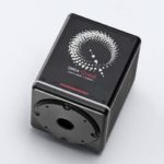
Hamamatsu Photonics introduces the world’s first photon-number-resolving scientific camera with incredibly low noise and 9.4 megapixels

Hamamatsu Photonics has designed and produced a scientific camera called the ORCA®-Quest qCMOSTM camera (part number C15550-20UP), having incredibly low noise of 0.27 electrons rms and a high pixel number of 9.4 megapixels. What makes this possible is a new Mehr

Hamamatsu Photonics will construct a new factory building at the Toyooka factory site to boost production capacity of its electron tube products

Hamamatsu Photonics will construct a new factory Building, No. 11, at its Toyooka factory site (Shimokanzo, Iwata City, Japan) to handle the increase in sales of Microfocus X-ray sources (MFX) and other electron tube products. The groundbreaking ceremony for the Mehr

Hamamatsu Photonics launches a new Webinar: qCMOS

This webinar with Peter Seitz, Ph.D., will provide an overview of semiconductor image sensors and introduce photon-resolving quantitative CMOS imaging (qCMOS). Wednesday, May 19th at 5:00pm CEST, 11:00AM EDT Register: https://www.hamamatsu.com/eu/en/news/event/2021/20210519190000.html About this webinar: Imaging in general and semiconductor imaging Mehr

Hamamatsu Photonics will construct a new factory building at the Joko factory site to boost production capacity of image measurement devices and equipment business

Hamamatsu Photonics will construct a new factory, Building No. 5 at the Joko factory site (Joko-cho, Higashi-ku, Hamamatsu City, Japan) to handle expanding sales of image measurement devices and equipment such as digital cameras for scientific measurement, digital pathology slide Mehr

Hamamatsu Photonics has developed laser thermal processing equipment capable of operating with a high degree of freedom

At Hamamatsu Photonics we have developed laser thermal processing equipment for laser quenching that combines a direct diode laser, (DDL) that we newly designed and developed based on our unique laser diode (LD) technology, with a 6-axis robotic arm capable Mehr
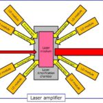
Hamamatsu Photonics has developed a high power QCL module

Hamamatsu Photonics have developed a high power QCL module that delivers an average output power of 2 watts at a wavelength of 8.6 micrometers (1 micrometer or μm is one-millionth of a meter). This high power QCL module was created Mehr

Hamamatsu Photonics has developed a high-sensitivity, high-resolution semiconductor failure analysis system that utilizes visible to near-infrared light, all in just a single unit

Hamamatsu Photonics has developed a new semiconductor failure analysis system called the “PHEMOS-X C15765-01” that in just a single unit utilizes visible to near-infrared light to analyze semiconductor defects. What makes this possible is a newly mounted multi-wavelength laser scanner Mehr